PCB Design with KiCad Part 6: symbol vs footprint — one part, two drawings

The symbol is how it looks in the schematic; the footprint is the copper pads it needs on the board (through-hole or SMD like 0805).
One resistor — so why does KiCad draw it TWICE? 🤔🟩
✏️ The SYMBOL lives in your schematic: it shows WHAT the part does and how it connects.
🟨 The FOOTPRINT lives on the board: the real copper pads (or holes) the part gets soldered to — WHERE it sits.
🔁 One symbol, many footprints:
• Through-hole: two holes 10.16 mm (0.4 in) apart → Resistor_THT:R_Axial_DIN0207…P10.16mm
• SMD 0805: a tiny 2.0 × 1.25 mm part on two flat pads → Resistor_SMD:R_0805_2012Metric
❌ Pick the wrong footprint and the real part won't fit your board!
✅ In KiCad: open the symbol's Footprint field, or Tools → Assign Footprints.
Read the voiceover (transcript)
- One resistor. Why does KiCad draw it twice?
- The symbol shows what it does, in your schematic.
- The footprint shows where it sits: copper pads on the board.
- Same symbol, many footprints: big holes, or tiny pads!
- This one is tiny. Which footprint?
- Tiny pads: oh eight oh five!
- Wrong footprint? It won't fit!
- Next: from schematic to board. Follow for Part 7!
Related lessons
 EP.164 · PCB Design with KiCad · 4PCB Design with KiCad Part 4: Power symbols + net labels
 EP.228 · PCB Design with KiCad · 8PCB Design with KiCad Part 8: place parts like a pro
 EP.148 · PCB Design with KiCad · 3PCB Design with KiCad Part 3: Your first schematic — battery, resistor, LED
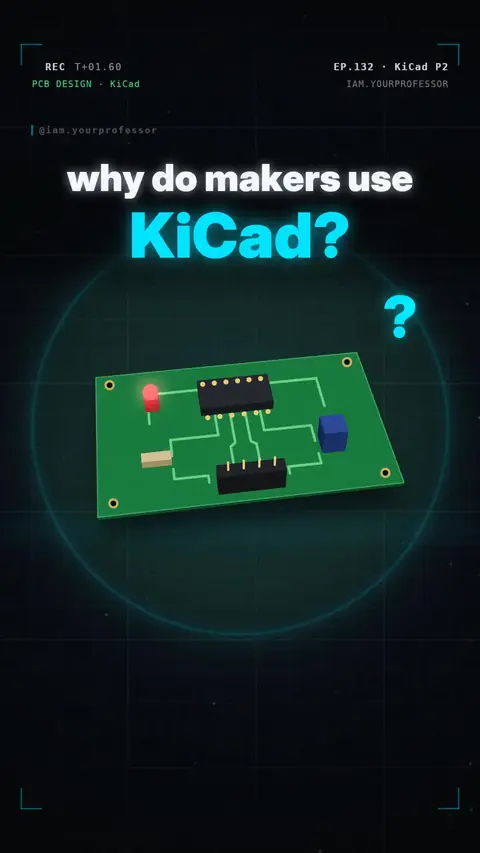 EP.132 · PCB Design with KiCad · 2PCB Design with KiCad Part 2: Why KiCad?
Get new lessons + early access to the full course
One email when new lessons drop. No spam, unsubscribe any time.
✓ You're on the list! We'll email you when new lessons drop.
By joining you agree to the privacy policy.