PCB Design with KiCad Part 7: from schematic to board — ratsnest and board outline
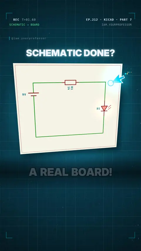
// WHAT YOU WILL LEARN
Update the PCB from the schematic: thin ratsnest lines show what must connect; draw the board shape on Edge.Cuts.
// LESSON NOTES
Schematic done? Now make it a REAL board! 🟩🛠️
⌨️ In the KiCad PCB Editor press F8 (Tools → Update PCB from Schematic).
📦 All your footprints land on the screen, tied together with thin lines.
🕸️ That's the RATSNEST: it shows which pads must be connected (you'll draw copper tracks over them later).
🤔 But where does the board end?
✏️ Draw its shape on the Edge.Cuts layer (the yellow one).
✂️ That line is exactly where the board factory cuts.
Read the voiceover (transcript)
- Schematic done? Now make it a real board!
- Press F8: update the PCB from the schematic.
- Your parts land, tied together with thin lines.
- That's the ratsnest. It shows what must connect.
- But where does the board end?
- Draw it on Edge Cuts!
- That line is where the factory cuts.
- Next: place your parts like a pro. Follow for Part 8!
Related lessons
 EP.180 · PCB Design with KiCad · 5PCB Design with KiCad Part 5: ERC — let KiCad find your wiring mistakes
 EP.164 · PCB Design with KiCad · 4PCB Design with KiCad Part 4: Power symbols + net labels
 EP.148 · PCB Design with KiCad · 3PCB Design with KiCad Part 3: Your first schematic — battery, resistor, LED
 EP.132 · PCB Design with KiCad · 2PCB Design with KiCad Part 2: Why KiCad?
// NEWSLETTER · FREE
Get new lessons + early access to the full course
One email when new lessons drop. No spam, unsubscribe any time.
✓ You're on the list! We'll email you when new lessons drop.
By joining you agree to the privacy policy.