PCB Design with KiCad Part 1: What is a PCB?
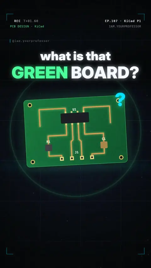
A board of fibreglass (FR-4) with copper tracks instead of wires, a coloured solder mask on top and white silkscreen labels.
What is that green board inside every gadget? 📱💻 Here's how it works 👇
1️⃣ IT'S A PCB — a Printed Circuit Board. Thin copper paths replace all the messy wires, so the circuit is neat, small and the same every time.
2️⃣ 4 LAYERS: a fiberglass core (FR-4), thin copper tracks (about 0.035 mm!), a green solder mask that protects the copper, and white labels (silkscreen) like R1, C1, U1. Most boards have copper on both sides.
3️⃣ MAKE YOUR OWN: you can design one for free in KiCad (Windows, macOS, Linux), send the files to a PCB maker, and they build it and post it to you.
Board, copper, mask, labels!
New series: PCB Design with KiCad — from your first schematic to a real board in your hands.
Read the voiceover (transcript)
- What is that green board inside every gadget?
- It's a PCB, a printed circuit board! Copper paths replace all the messy wires.
- Inside: a fiberglass core, thin copper tracks, a green solder mask, and white labels.
- You can design one for free in KiCad, and a PCB maker builds it for you!
- Board, copper, mask, labels!
- Next: why KiCad? Follow for part two!
Related lessons
 EP.105 · Embedded C · 6Embedded C Part 6: What is a register?
 EP.110 · Maths for Electronics · 13Maths for Electronics L13: Radians — why 360° = 2π
 EP.102 · Home Electrical · 9Home Electrical Part 9: Hybrid inverter — solar, battery and grid in one box
 EP.113 · LED Series · 12millis() vs delay(): blink without freezing
Get new lessons + early access to the full course
One email when new lessons drop. No spam, unsubscribe any time.
✓ You're on the list! We'll email you when new lessons drop.
By joining you agree to the privacy policy.